SEM/EDX
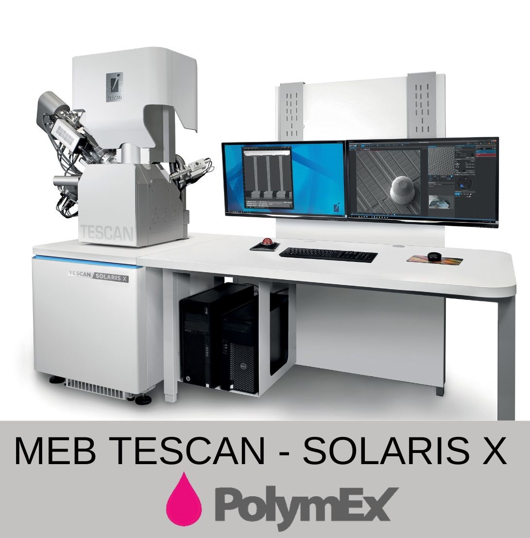
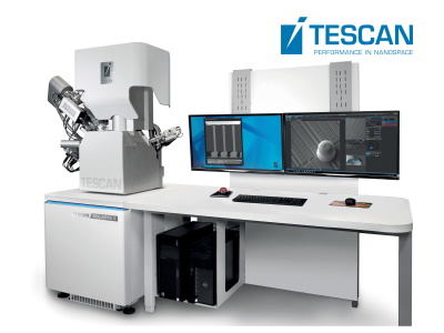
Equipment : Scanning Electron Microscope - SOLARIS X and SEM-FIB Plasma/Gallium +EDX-EBSD
Detection modes available :
- SE: Secondary electrons with topography contrast.
- GSE: Secondary Electron Gas (presence of water vapour).
- BSE: Backscattered electrons with chemical contrast (heavy elements in light on the BSE images)
Sample : 8" max., 130 mm X & Y
Resolution : 0.5nm@30kV
Application domain
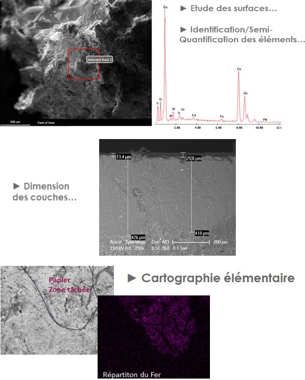
- Surface study (defects ...),
- Polished section study (load sizing, layer thickness, etc.),
- Characterization of materials (elemental analysis of all elements) ...
- Biology: Until now, the vacuum constraints imposed by scanning electron microscopy (the electrons must be accelerated under a high vacuum) constituted a handicap for many applications. For example, biological samples, hydrated, oily or insulating products that require observation in their natural state.

 EN
EN
 FR
FR